Although the use of atomically thin materials rather than silicon as the foundation for new transistors is fascinating, connecting such ‘2D’ materials to other traditional electronic components has proven tricky. Researchers at MIT, the University of California at Berkeley, the Taiwan – Based Semiconductor Company, and other institutions have devised a method of creating these power cables that could assist to unlock the potential of 2D materials and advance component miniaturization— possibly enough to extend Moore’s Rule, at least for the time being. Further advancements in this field will be researched and updated in the blogs by the top engineering college in Coimbatore. The composite 2D materials or films, which are just a few electrons wide, satisfy all of the requirements for shrinkage, possibly decreasing the channel length, which is now approximately 5 to 10 nanometres in trimming chips, to a sub-nanometer range.
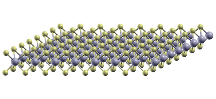
There is no energy barrier for the electron to pass through at the interface between the semimetal (bismuth) as well as the 2D semiconductor (MoS2), resulting in extremely low electrical resistance among them. Read more about the latest trends in the field of Electronics and Communication Engineering by the Top Electronics & Communication Colleges In Tamil Nadu